Logical effort
|
|
The method of logical effort, a term coined by Ivan Sutherland and Robert Sproull in 1991, is a straight-forward technique used to estimate delay in a CMOS circuit. Circuit topology and gate sizing are key components utilized in this method.
Logical effort helps us answer questions such as the following:
- For a given function, which gates should be used?
- How should a combinational logic network be designed to obtain minimum delay?
- How many levels of logic are correct for a circuit?
- How can symmetric rise and fall time be obtained?
- What is the minimum transistor sizing needed to drive a given load capacitance?
| Contents |
Derivation of delay in a logic gate
Delay is expressed in terms of a basic delay unit, τ = RC, the delay of an inverter driving an identical inverter with no parasitic capacitance. The absolute delay is then simply defined as the product of the delay of the gate, d, and τ:
- <math>d_{abs} = d\tau<math>
The unit of delay is therefore measured relative to τ. In a typical 0.6 micrometre process τ is about 50 ps. For a 0.25 micrometre process, τ is about 20 ps.
Alternatively, delay in a logic gate can be expressed as a summation of two primary factors: parasitic delay, p, and stage effort, f. Consequently,
- <math>d = f + p<math>
The stage effort can be further divided into two components: a logical effort, g, which captures the intrinsic properties of the gate, and an electrical effort, h, which describes the load. The stage effort is then simply:
- <math>f = gh<math>
while the electrical effort is calculated via:
- <math>h = \frac{C_{out}}{C_{in}}<math>
Combining these equations yields a basic equation that models delay through a single logic gate, in units of τ:
- <math>d = gh + p<math>
Delay in an inverter
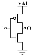
The logical effort of an inverter is defined to be g = 1 by noting that the input capacitance of a minimum size inverter has an NMOS input capacitance of 1, while the PMOS input capacitance is two. Thus g = 3/3, and g = 1. Remember: electron mobility is greater than hole mobility.
The parasitic of an inverter is p = 1. If γ = 2, and the inverter drives an equivalent inverter, then:
- <math>d = gh + p = (1)(1) + 1 = 2<math>
Delay in a NAND gate
The logical effort of a two-input NAND gate is calculated to be g = 4/3. A NAND gate is typically preferred to NOR as a result of its lower logical effort.
"Intrinsic properties" of a circuit
Basically it is equivalent/normalized RC value at input.
A simple multi-stage inverter sizing problem illustrates the idea:
http://bwrc.eecs.berkeley.edu/Classes/IcDesign/EE141_s02/Lectures/Lecture7-invsize.PDF
See also
- Sutherland, Ivan E, et. al. Logical Effort: Designing Fast CMOS Circuits. 1999.

